
Silicon has traditionally been viewed as the very essence behind modern technology to make it digital in its true sense. From microchips in cell phones and computers to solar energy systems, this versatile element acts as an industrial workhorse. One of the silicon properties that hugely influences its behaviour in various applications is density. This blog aims to explore the density of silicon, unveiling its physical properties, why it matters in technological developments, and how it is forging new avenues for the future. Techies, scientists, and even just inquisitive minds will find enlightening information in this post about how silicon amazingly shapes our world.
Introduction to Silicon
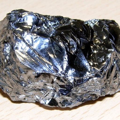
Silicon is a chemical element with the symbol Si and atomic number 14. It is hugely abundant on Earth, found chiefly in sand and quartz. Having a density of approximately 2.33 grams per cubic centimeter, silicon is lighter than many metals but is structurally solid. Being capacitor by definition, silicon makes electronics possible and is thereby used in the production of computer chips and solar panels. The combination of abundance, durability, and semiconductor ability is silicon’s great uniqueness and the reason that it is deemed an essential resource for contemporary technology.
Importance of Silicon in Industries
The versatility of silicon has made it relevant in various industries. The global semiconductor industry heavily depends on silicon-based wafers for fabricating integrated circuits and microchips, which are the basic hardware components of computers, smartphones, and other electronic appliances. From recent market data, it can be gleaned that the semiconductor industry stood at a valuation of approximately $600 billion in 2022, with silicon being the very backbone of this booming industry.
Silicon is of paramount importance for solar energy in renewable energy sectors. In production of photovoltaic (solar) panels, silicon is used as a key material to convert sunlight efficiently into electricity. It is estimated that more than 90% of solar panels produced in the world employ silicon-based technologies, which attests to its centrality in clean energy transition.
The construction industry and the automotive industry also gain from silicon. In these industries, silicone rubber and silicon-based sealants provide superior thermal stability and flexibility against environmental weathering. For example, silicones contribute to the automotive sector by enhancing the performance and durability of engine hardware, electronic systems, and safety mechanisms.
The newer development of silicon anode technologies in batteries shows promising quickening in bringing about high-capacity energy storage. Studies indicate that silicon-based batteries can be as much as ten times more energy-dense than current commercial lithium-ion batteries, which would be utterly transformational for the development of electric vehicles and portable gadgets.
From its ability to improve manufacturing to energy innovation, silicon’s presence in all industries attests to its paramount role in evolving technology in the present age.
Silicon Properties Outline
The chemical element silicon is denoted by the symbol Si and has an atomic number of 14. It is considered a metalloid, possessing certain properties suggestive of metals while bearing nonmetal properties as well, rendering it very versatile. The key property that distinguishes it is that of a semiconductor wherein it under specific conditions it passes current and under other conditions it resists the passage of current. This property is important for its application in electronic devices, particularly transistors, and integrated circuits.
Silicon is also very abundant, making about 28% by weight of the Earth’s crust, thus, constituting the second most abundant element after oxygen. It mostly occurs as silicon dioxide (SiO₂) and silicate minerals, which industries value in construction and glass-making. For instance, global production of silicon metal reached around 8 million metric tons in 2022, driven by demand in industries ranging from construction to electronics.
Its thermal stability and corrosion resistance also help its usage in high-temperature places. This property is amply demonstrated in solar panels, where silicon gains the greatest depreciation of light as well as durability to allow photovoltaic cells to convert up to a considerable level of light into electric power. Monocrystalline silicon solar panels, as per recent data, have energy efficiency levels of their own up to 22 percent best, while the rest of the considered solar technologies lag behind.
These marvels of silicon keep it ultimately at the core of cutting-edge technologies and thus in another way, its destiny establishes concepts for ongoing entrepreneurial opportunities.
Silicon in Electronics and Photovoltaic Technologies
Silicon still represents the singularity of electronics and solar energy technology developments. Making optimum use of its semiconductor behavior, silicon has become the material of choice in integrated circuit, transistor, and microchip manufacturing, which constitute the backbone of modern electronics. Over 90% of the electronic devices produced in the world today have integrated circuits made from silicon; hence, it is truly the driving force behind innovations in smartphones, laptops, and advanced computing systems.
While in the solar energy segment, silicon still remains unchallenged as the mainstream material source for photovoltaic cells thanks to its general abundance, durability, and efficient photoelectric conversion of the major drain on black resources. The monocrystalline silicon solar cell, which is the best silicon solar panel form, has been reported by NREL to have recorded efficiencies in excess of 26.8% in the laboratory. More than 20-22% of efficiency is usually guaranteed for commercial applications of these solar panels, outperforming other materials such as polycrystalline silicon and thin film culture.
Besides, improvements in silicon solar technology like the passivated emitter rear cell (PERC) have considerably enhanced module performances by cutting back energy losses. Ongoing research aims to beat 30% efficiency through tandem cell technology, coupling silicon with complementary materials abstractions like Perovskite. The ease of processing and scalability of silicon gives it a central position in the renewable energy landscape and offers a path to a sustainable future.
They are using silicon not only to improve existing applications but also to make a great leap toward the next-level inventions in electronics and renewable energy worldwide.
Density of Silicon

Silicon has a density of about 2.33 grams per cubic centimeter (g/cm³). The density being so low, the material is quite lightweight compared to metals and hence is widely utilized in industries related to electronics and solar energy systems.
Atomic Structure and Its Correspondence with the Density
One interesting effect of the atomic arrangement of silicon is the physical property of the material such as density and functionality. Silicon has an atomic number of 14 with an atomic mass of approximately 28.09 amu. The atoms crystallize in a diamond cubic arrangement, or simply a tetrahedral arrangement, contributing to its stability and, consequently, versatility in many technology applications.
Of course, silicon has a density at room temperature of approximately 2.33 g/cm³ and depends to a larger extent on temperature changes. With an increase in temperature, silicon atoms vibrate with greater amplitude, creating a more expanded volume and low density. This property is, therefore, very important in the manufacture of semiconductors, whereby silicon wafer handling must undergo very accurate thermal control.
More recent data show that global silicon production is increasing at a frantic pace to satisfy the needs for electronics and solar panels. Market reports indicate that over 8.5 million metric tons were produced in 2022, and new approaches to refining allow for the purity of up to 99.9999% in semiconductor-grade material. This shows how important it is to understand silicon with respect to the atomic and physical properties that help the development of high-tech industries.
Crystalline Structure of Silicon
Silicon crystallizes in the diamond cubic crystal structure, a form that determines, to an important extent, its physical and electronic properties. The silicon atom is covalently bonded to four neighboring silicon atoms, setting up a tetrahedral lattice. This arrangement generates an extremely stable structure having a bandgap of almost 1.1 eV, which is then conducive to the importance of silicon as the original device material.
Recent studies have underlined the developments targeting improvements of silicon crystalline perfection, given the importance of its application in present-day technologies. Monocrystalline silicon is touted as the most efficient material used in photovoltaic cells and microelectronics due to the uniform arrangement of atoms. Data published in 2023 indicated that the worldwide market for monocrystalline silicon wafers had crossed $60 billion, with a forecasted growth of more than 10% per annum, stemming from the increasing application in solar energy systems and high-performance processors.
Further development in crystal growth methods such as the Czochralski process and Float Zone technique allow production of silicon with a reduced level of impurities and dislocations. Such development speaks for the continuous development aimed at improving the crystalline structure of silicon for applications at the forefront.
Comparison of Silicon Density with Other Materials
Silicon’s density is approximately 2.33 g/cm³, which is lower than metals like aluminum (2.70 g/cm³), iron (7.87 g/cm³), and copper (8.96 g/cm³), but higher than materials like plastic (~1.00 g/cm³) and glass (~2.20–2.60 g/cm³).
| Material | Density (g/cm³) | Comparison |
|---|---|---|
| Silicon | 2.33 | Baseline |
| Aluminum | 2.70 | Higher |
| Iron | 7.87 | Much higher |
| Copper | 8.96 | Much higher |
| Plastic | ~1.00 | Lower |
| Glass | 2.20–2.60 | Comparable |
Its actual and potential applications in practice: Silicon density

The density of silicon is approximately 2.33 g/cm³. So in cases where phenomena require strength and lightweight features, silicon is used. It can be synthetically manufactured in a wide variety of computer chips, integrated circuits, and electronic components by the semiconductor industries. This density enables small and lightweight designs to be very efficient. Anyhow, since silicon is a bit denser than glass, it finds applications in solar panels, providing resilience without too much burden.
Silicon Wafers: Backbones in Semiconductor Manufacturing
For the fabrication of microchips and integrated circuits, silicon wafers stand to be nowadays immensely common in the manufacturing of semiconductors. These very thin cuts of semiconductor material are usually produced using silicon crystals with low impurities for enhanced performance. After gaining popularity since the creation of the first fabrication processes and the development of fabrication tools, the sizes of silicon wafers have evolved through time, with most modern fabrication facilities running usually 300mm (12-inch) wafers and a few with advanced process development facilities already prepping for 450mm (18-inch) wafers to enable better throughput and cheaper chips.
The various steps and approximate orders refer to the production process from raw silicon to wafers, consisting roughly of purification from metallurgical-grade silicon to electronic-grade silicon with a minimum purity of 99.9999999% (9N purity), crystal growth from this electronic-grade silicon through the Czochralski (CZ) or Float Zone (FZ) method produces large single crystals, slicing of crystals into thin wafers, polishing of wafers for mirror-like surface, and very thorough cleaning of silicon wafers from even molecular contamination.
According to several industry-specific sources, the global silicon wafer market is expected to exceed $15 billion in revenues by 2025, fueled by the rising demand for consumer electronics, data centers, automotive electronics, and 5G technology. Moreover, cutting-edge lithography and transistor design have pushed the silicon wafer technology to its limits, with nanometer-scale features presently etched on these silicon wafers to come up with state-of-the-art chip designs. Constant innovation thus ensures that silicon wafers remain ever essential towards modern technological development.
Importance of Density in Silicon-Based Products
Consider that the density of transistors on one silicon wafer is extremely relevant to the total activities being carried out by the transistor under test and hence power optimization and cost-effectiveness of the semiconductor device. From some recent industry information, new 3 nm node fabrication advances made by the likes of TSMC and Samsung greatly enhanced transistor density. These 3 nm chips are said to be packing about 300 million transistors per square millimeter, a major improvement from all earlier generations, therefore speeding up processing speeds and lowering energy consumption.
In the same context, enhanced transistor density implies more complicated and powerful chips can be designed within the same physical footprint. As an example, with these high-density designs, modern processors are now capable of integrating exceedingly complex AI functions directly on-chip. Also, Gartner projects that the global semiconductors market would cross the $600 billion mark by the year 2024, principally aided by the demand for these high-density chips in applications such as autonomous vehicles, cloud computing, and IoT.
This process is made possible by the use of technologies like Extreme Ultraviolet Lithography (EUV), which provides the accuracy needed to fabricate these densely packed and highly optimized semiconductor devices. As this technology is improved further, transistor densities are projected to double every two years, as per the fundamental predictions of Moore’s Law, although the challenges to achieving this from a smaller dimension are going to require some real innovative engineering.
Importance of Silicon Dioxide for Industry
An abundance of unique qualities makes silicon dioxide (SiO₂), commonly known as silica, a primary raw material across a wide range of industries. It is an essential industrial material, mainly in the semiconductor industry, where it is used as an insulator and, to a lesser extent, in the preparation of silicon wafers. The high thermal stability and dielectric strength of silicon dioxide make it ideal for these applications. For instance, SiO₂ is used extensively in modern electronics as a passivation layer to protect semiconductor surfaces from contaminants and mechanical stress.
It also highlights the importance of its use in chip production through recent research. The silicon wafer market, in which the fabrication of silicon wafers depends heavily on silicon dioxide, was valued at about 11.6 billion dollars in 2021 and is expected to grow at a 5.6% CAGR until 2026, based on reports by the MarketsandMarkets. And, the demand that is growing for SiO₂-based nanoparticles in coatings, optical devices, and composite materials highlights the versatility of those applications.
Beyond electronics, silicon dioxide is crucial for construction, being a major ingredient in cement and glass production. Because this material is too abundant in nature, making up over 59% of the Earth’s crust, it is securely supplied for industrial use. New applications of SiO₂, such as energy storage and sustainability materials, are explored by nanotechnology, which highlights how relevant SiO₂ is in applied engineering today.
Recent Research and Technological Advancements
SiO₂ is captivating research interests towards applications in renewable energy and environmental sustainability. Key aspects include the enhancement of solar panel efficiency and the use of SiO₂ with other high-performing battery materials in energy storage. Other aspects of its examination are oriented toward the use of SiO₂ in water purification due to its filtering ability. Such scenarios furthermore demonstrate the versatility and modern-day application potential of SiO₂ in tackling present technological and environmental challenges.
Advances in Silicon Density Measurement
The recent advancements in silicon density measurement have tremendously developed precise and efficient material analysis for various industries. Scientists and engineers are applying avant-garde techniques such as X-ray diffraction (XRD), optical interferometry to measure with utmost precision the density and structural properties of silicon. A remarkable development is the use of digital holographic microscopy (DHM) which provides nanometer accuracy in density measurement by capturing the three-dimensional structure of silicon.
Advances are also progressing in computational modeling, allowing simulations of silicon microstructures useful in enhancing the understanding of density variability under different conditions. For example, experimentation pointed out that fine-tuning silicon density can be instrumental in improving semiconductors and photovoltaic cells. Recent investigations affirm that increasing uniformity and reducing defects in silicon’s atomic structure enhance energy conversion in solar panels by approximately 5%.
Further, precise density measurements are important in manufacturing silicon-based components, where slight variations can result in performance disparities. When merging these state-of-the-art measurement techniques with automated production lines, the manufacturers ensure high efficiency and quality control, cementing silicon’s position as a key base material in modern technology.
Recent Findings in Silicon Applications
Recent advancements in silicon applications have endowed remarkable breakthroughs across diverse industrial sectors. For example, recent research reveals that silicon carbide is getting increasingly utilized in electric vehicle production due to its superior energy consumption efficiency. According to a report by Yole Intelligence published in 2023, SiC semiconductor market revenue is expected to grow from $1.5 billion in 2021 to over $6 billion by 2027, mainly driven by the demand for EVs and renewable energy systems.
Further innovations lie in the use of silicon in battery technologies. Silicon anodes are set to challenge graphite anodes in lithium-ion batteries as they are capable of storing discharges up to 10 times more. It is alleged that companies, including Tesla, are adopting silicon in their EV batteries to optimize energy density and vehicle range. A 2023 study published by Nature Communications states that with further optimization of silicon anode design, battery lifetimes may be enhanced by 20%, establishing a new standard for energy storage systems.
The latest silicon photonics will enormously benefit the field of microelectronics. It takes advantage of silicon optics to facilitate faster data transmission in telecom and data center lands. Recent IEEE publication shows silicon photonics supporting data rates of more than 400 Gbps that resolve the issue of demand in growing high-speed internet and cloud computing services. These advanced technological breakthroughs magnify silicon’s criticality in orchestrating futuristic technology.
Effects of Density on Silicon-Based Technologies
With time, the introduction of varying densities in transistors and circuits in silicon-based technologies has been the factor for upgrading computational power and efficiency. Since, with respect to chip design, Moore’s law deals with the fact that the number of transistors doubles every two years; advances in silicon fabrication technique have greatly supported this prediction. A higher density leads to a set of processors, implemented more energy-efficiently, with a smaller physical area in modern devices.
This is the kind of density enhancement that recent 3 nm process technologies debugged at TSMC and Samsung have Technically crafted by introducing over 300 million transistors for every square millimetre, wherein a direct impact of this density enhancement allows a further 15% enhancement in speed and around 30% enhancement in power efficiency as discretized by 3G transistor density on performance. These developments will enhance further for the implementation of artificial intelligence, machine learning, and high-performance computing.
At the same time, there are roadblocks to greater density, like maintaining signal integrity and heat dissipation. The research community is in trials for new materials such as 2D semiconductors and advanced cooling solutions to get past the limitation. Simultaneously, 3D integrated circuits (3D ICs) are gaining adoption to address spatial constraints by stacking multiple layers of silicon in a compact multi-layered configuration for further enhancement of functionality.
This pursuit of higher density is constant evidence for the semiconductor industry’s spirit of mitigation and innovation as a guarantee for silicon-based technologies to remain relevant in a digitally interconnected world.
Future Developments in Silicon Density
As I see it, the future in silicon density lies with breakthroughs in materials science, advanced lithography techniques, and novel architectures such as 3D ICs. These discoveries will be critical in overcoming present restrictions to continue the pace of miniaturization and performance enhancement in the semiconductor industry.
Predicted Innovations in Silicon Materials
The next wave of the silicon-material innovation will involve materials science, in particular, silicon carbide and gallium nitride, for high-speed applications. Silicon carbide is gaining acceptance in power electronics because it can tolerate higher voltages and temperatures than conventional silicon. According to recent reports, SiC-based power devices could reduce energy losses by as much as 50% when compared to silicon-based technologies, thus making these critical for EVs and renewable energy systems.
Furthermore, materials such as gallium nitride are expected to become more dominant in high-frequency applications such as 5G infrastructures, radar, and satellite communications. According to the research done by industry analysts, the global market for GaN semiconductor devices is expected to grow with a CAGR of more than 20% between 2023 and 2030, implying its growing importance.
On the other hand, advances in doping techniques and new composite materials, such as silicon germanium alloys, will push silicon’s potential even further. These advances will not only increase the density of transistors but will also increase conductivity and thermal management, which are very important factors when scaling semiconductor technologies. This strength will be needed to overcome the limits placed by Moore’s Law with extremely high-performance efficiency in next-generation devices.
Potential Impacts on Technology and Industry
The potential advancement in the field of semiconductor materials and technologies is expected to take the whole technology landscape into a new shape. According to a recent report from McKinsey, semiconductor industry will by that time exceed $1 trillion market value in 2030, driven by the demands of AI, machine learning, and 5G technologies.
Silicon-germanium alloys allow higher electron mobility for approximately 30 percent improvement in transistor efficiencies, thus making them appropriate for high-speed communication devices, quantum computing, and advanced sensing applications, source IEEE Spectrum. Besides, the new fabrication technologies such as EUV lithography allow the manufacture of sub-3nm transistor scales and thereby increase transistor density.
Indeed, these improvements will also help buildings in medicine, automotive, and consumer electronics. For instance, connected medical devices powered by semiconductors would improve diagnoses and patient outcomes. On the other hand, autonomous vehicles will heavily rely on supercomputers to process vast data in real time.
These evolutions also consider energy efficiency, with modern semiconductors halving data centers’ energy consumption. That is why it is critical to achieving sustainability in energy-heavy industries without compromising their performance.
Environmental Considerations of Silicon Density
An ever-growing silicon density within modern semiconductors has, above all, given environmental advantages, but at times it poses challenges. From available data, progress in chip design has led manufacturers to host increasing transistors per smaller area, thus improving speed and power efficiency. Transitioning slight from 7nm to 3nm process technology was able to bring about at least a 15% enhanced performance while power consumption was reduced by as much as 30%, as rated by industry leaders such as TSMC and Samsung.
On the other hand, the making of an advanced high silicon density chip would easily gulp huge levels of energy and natural resources. An analysis done in 2023 revealed that producing just a single advanced chip would consume in excess of 2,000 liters of ultrapure water while generating about 40 kg-C02 as its carbon footprint. These points highlight the urgent need for the semiconductor industry to adapt to eco-friendly practices: recycling water used in production or searching for substitute materials that are less dependent on rare earth metals. Balancing the benefits of increasing silicon density with environmental responsibilities has remained in the minds of the researchers, as well as the manufacturers.
Reference sources
1. Density of Silicon Crystals
-
- Authors: M. Tanaka, A. Peuto
- Journal: Metrologia
- Publication Year: 1994
- Citation Token: (Tanaka & Peuto, 1994, pp. 219–230)
- Summary: This paper reviews measurements of silicon crystal density for the determination of the Avogadro constant. It discusses volume, mass, and hydrostatic-weighing measurements, focusing on error sources and measurement uncertainty. The outlook on achieving experimental uncertainties of less than 10−7 is described, emphasizing the need to reduce uncertainty sources arising from surface conditions, such as silica layers and damaged crystalline layers.
2. Comparative Study on the Effect of Magnetic Field on the Photocurrent Density of Organic, Dye-Sensitized, and Silicon Solar Cells
-
- Author: H. Fathabadi
- Journal: Journal of Materials Science: Materials in Electronics
- Publication Year: 2019
- Citation Token: (Fathabadi, 2019, pp. 17314–17321)
- Summary: This study investigates the impact of magnetic fields on the photocurrent density of various types of solar cells, including silicon solar cells. The research highlights how external magnetic fields can influence the performance of solar cells, providing insights into optimizing their efficiency.
3. An Improved Methodology for Extracting the Interface Defect Density of Passivated Silicon Solar Cells
-
- Authors: Zheng Xin et al.
- Journal: IEEE Journal of Photovoltaics
- Publication Year: 2016
- Citation Token: (Xin et al., 2016, pp. 1080–1089)
- Summary: This paper presents a methodology for accurately determining the interface defect density in passivated silicon solar cells. The authors discuss the significance of interface defects on solar cell performance and provide a detailed analysis of their extraction methodology, which enhances the understanding of defect-related losses in solar cells.
Frequently Asked Questions (FAQs)
What is the density of silicon?
Experimental values for the density of silicon at room temperature is about 2.33 grams per cubic centimeter (g/cm³). This value tends to change slightly for different purities and crystallographic structures of silicon.
What is silicon density compared to other materials?
Silicon has less density when compared to heavy metallic elements such as iron-7.87 g/cm³, copper-8.96 g/cm³, yet it is more than many lighter non-metals, such as aluminum-2.70 g/cm³. This makes silicon an important material for applications like electronics and solar cells.
What are some factors that influence the density of silicon?
Changing temperature, pressure, or impurity in it affects the density of silicon. Another factor influencing density variation is the allotropes of silicon like amorphous and crystalline-related silicon.
What makes the density of silicon important in electronics?
Hence, in a semiconductor, the density aspect must be addressed. Thermal conductivity, mechanical strength, and the device’s operational performance are modulated by this material property for efficient circuits and devices.
How can the density of silicon be measured?
By use of Archimedes’ principle, by which it involves weighing the silicon sample when it is immersed in a liquid, or by using analytical balances and direct precision measurement of the silicon sample.
What are applications of silicon based on its density?
Owing to its density and its other physical characteristics, silicon finds its use largely in making semiconductor devices, photovoltaic cells, and other forms of instruments in the electronics field. Due to density, it provides structural integrity to the devices while keeping them just light enough to be effectively used.
Can the density of silicon change under extreme conditions?
Yes, the density of silicon can alter under extreme conditions such as high temperature and pressure. For example, in a high-pressure environment, silicon can undergo several phase transformations that lead to changes in density and other physical properties.
What is the significance of silicon density in solar panels?
The silicon density bears much significance in solar panels as it affects the very weight and efficiency of these panels. Lower density would then mean lighter panels that would be easier to install and transport, all while being sufficiently strong and conductive to carry out energy conversion.
